![]()
![]()
![]()
![]()
NBI Generation 3 Array Controller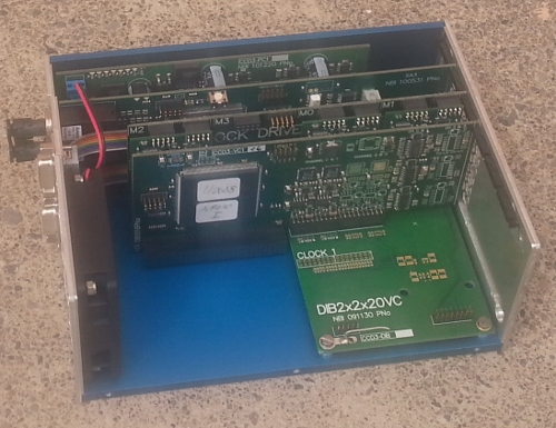
IntroductionThe generation 3 array controller is the latest in a series of controllers developed at NBI in Copenhagen. The most redeeming feature of this new unit is that it is all digital, i.e. it uses digital correlated double sampling and digitally derived clock waveforms. As a result the controller is small, uses little power and is very flexible to programme, but retains all the low noise performance of the previous generations. The whole controller, with internal power supply, fits in a single box some 18x13x7cm in size. External power can be derived from a 50W, 24V dc switch mode power supply. Typical power consumption for operating a two channel CCD is ~24W.The controller comes with its own data acquisition system called ccd3comm, which provides a complete user interface, under Linux, for setting up and operating the controller, acquiring data, displaying images and producing standard FITS files. It is possible to run external shell scripts or batch files within ccd3comm. A comprehensive set of commands have been written, that can be used to modify anything from the clock waveforms, to setting the bias voltages and configuring the detector read format e.g. define windows and reading back telemetry information. The controller consists of the traditional series of boards, a power supply for producing all the various voltage rails required for both bias and clocking, a sequencer board based around an Altera FPGA, a digital clock driver board and finally a video board. Communication with the controller is over a duplex fibre optic link to a custom PCI (or soon to be provided PCIe) interface board in the data acquisition computer. All control logic for the PC interface card is contained in a FPGA and there is space for up to 1GByte of DDR-DRAM, to act as a frame store. The optical fibre connection between the host PC and the controller(s) can be either point to point or configured in a daisy chain, using the built in OptoRing communication system.
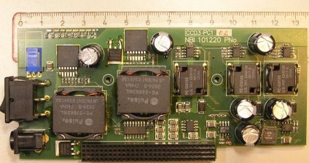
Power Supply
The power supply takes a 24Vdc input at up to 2.2A and converts it, by means of six switching regulators to the various bias and digital voltages required for the electronics. The switching regulators are synchronised to the pixel clock to eliminate switching noise on the readout. The board supplies high current low voltage logic voltages of 3.3V and 5V as well as low power -5V, +/-15V and 29V for the analogue circuitry, clocks and bias signals respectively.
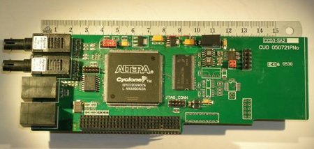
Sequencer Board
This is the main board in the controller, it is based around an Altera Cyclone FPGA and contains a 32-bit RISC Nios processor with SDRAM and flash memory. The main clock frequency is 80MHz so every operation is executed at a 12.5ns resolution. The sequencer board handles all the housekeeping, communication, sequencing, general control and synchronization.
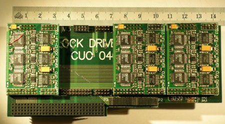
Clock Drivers
The clocking board consists of a carrier board which can accommodate up to four driver modules. The standard driver module contains six drivers which are made up with a 12-bit DAC updated every 12.5ns and an amplifier to a bi-polar output. The output is capable of delivering a voltage from -10V to 11.95V at 900V/us with a bandwidth of about 30MHz. Virtually any kind of waveform can be generated by these drivers, the patterns can be either generated by a local processor or uploaded from the host PC. It is possible to produce up to 96 clocks, when the maximum of four carrier boards are installed. It is foreseen that modules capable of producing high voltage EMCCD signals and ones for SWIR arrays will be available.
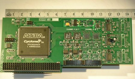
Video Board
A video board can support four video channels, with each channel consisting of a digital CDS path and bias generators to make typical voltages for VOD , VRD, and VRG. Up to four boards (16 video channels) can be accommodated in a single controller. The analogue CCD video signal first passes through a dual FET input differential amplifier before been digitised by a 14-bit ADC at 80MHz, which is directly coupled to a FPGA digital CDS processor. The input noise performance is 2 - 2.5 µV/√ Hz . Any type of CDS is possible to be programmed, dual-slope has been implemented with fixed value coefficients, i.e. no weighting. There are several stages in the CDS chain, including the possibility to apply a different gain to each channel to ensure similar gains for all channels, the dual-slope is applied and a resulting unsigned 32-bit pixel value transmitted. The controller by default provides four pixel speeds, 112kHz, 200kHz, 400kHz and 800kHz, though any reasonable speed can be derived by suitable adjustments of the timing.
ccd3comm Data Acquisition SystemThe DAS, ccd3comm runs under GNU/Linux and provides a complete interface for the controller, including a status window, a DS9 image display and a command window. Normally a controller will be delivered with a pre-installed and configured computer to the customer's specifications.The package includes a user editable configuration file ccd3comm.conf for customisation of the ccd3comm module, for example image display preferences and default FITS header parameters. ccd3comm has a low level command interface where commands can be issued. The program produces standard FITS image files and has the ability to include complete header information on the associated instrument status, for example through a data base interface. The user interface is implemented as a console program that reads from StdIn and writes on StdOut, thus ordinary piping and redirection can be used. This gives the user the ability to produce their own top layer that communicates to ccd3comm though these simple pipes. For example external shell scripts can be written, and piped to the DAS for execution. As an alternative to shell scripts, batch files can also be used. A batch file can be executed either from within ccd3comm by simply typing its file name or as an argument to ccd3comm, e.g. "ccd3comm -b [filename]".
An example of a batch file is given below: |
||
|